|
|
Electronic and geometric structure of the wurtzite GaN(0001) Surface |
![]()
|
Comparing different band structure calculations of wurtzite
GaN, the energetic positions of critical points differ by up to 0.8 eV.
To solve this discrepancy, angle resolved ultraviolet photoemission might be
applied, which is a powerful tool
for examining the electronic structure. Since the photoemission
process involves the excitation to outgoing scattering states, a full
account of the experimental data can only be attained by a comparison
with photocurrents calculated within the one-step model. Combined with a detailed theoretical analysis, photocurrents present also information about the geometrical properties of the surface. The GaN(0001) surface is expected to be stabilized by metallic bonds, an unusual behaviour compared to common III/V semiconductors as GaAs. Identifying these bonds in the theoretical spectra, the geometric and electronic structure can be tightly connected with the measured photocurrents. Figure 1 shows the bulk band structure of GaN in that direction relevant for normal emission from the (0001) surface. The two presented bulk band structures are adjusted to band structures of Vogel et al. and Rubio et al. They differ by their valence band width of 7.2 and 8.0 eV respectively.
|
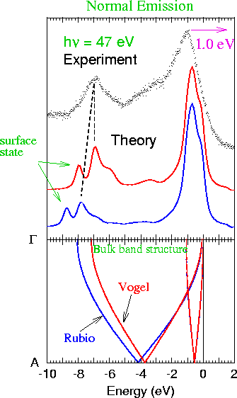 |
Fig. 1: The bulk band structures according to Vogel et al. and Rubio
et al. together with the respective photocurrents in normal
emission. The photocurrents are compared with experimental
results by Desi et al. The experimental data are shifted by
1.0 eV to lower binding energy.
|
|
On the top, Fig. 1 presents two calculated spectra in normal
emision, belonging to the above mentioned band structures.
The photon energy is chosen as 47 eV. For this excitation energy emissions
from the lower valence band edge can be expected, as has been checked by
structure plots.
Above the theoretical spectra an experimental result by Dhesi et al. is
shown. The experimental data are shifted by 1.0 eV to lower binding
energies. The necessity of this shift is conspicuous if one compares with a
whole series of spectra (photon energies from 31 up to 78 eV).
We explain
this difference by failures in the experimental determination of the valence
band maximum (VBM) by extrapolation of the leading edge. The comparison with experiment shows two points:
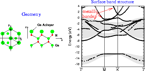
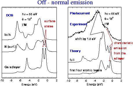
Fig. 2: The geometry of the GaN(0001)-(1x)Ga surface and the surface band structure. Figure 3 shows the density of states (DOS) and the theoretical photocurrent for an emission angle of 18 degree. For this configuration emissions from the M point are expected. The theoretical photocurrent shows two strong emissions between -1.0 and 0.0 eV. These emissions are related to the metallic surface states and are localized in the first atomic layers. This is checked with the layer resolved photocurrent, which is shown for the first four atomic layers. In addition to the theoretical results experimental photoemission data are shown.
Fig. 3: The density of states for different layers and the photocurrent for off-normal emission near the M-point. Also an experimental result by Dhesi et al. and the partial photocurrent of the first four atomic layers are shown.
The comparison with experiment leads to emphasize the following points:
Acknowledgment:
This work was supported by the BMBF under contract no. 05 SB8 FKA7.
|
1999 Thomas Strasser
![]()
 |