
|
|
Calculated optical potential and electron escape depth |
![]()
|
Damping of the electrons is an important feature in electron spectroscopy.
Usually it is treated with rough approximationson an empirical basis.
Here, for the
first time charge density functionals and GW calculations are applied
to quantitatively obtain these many-particle effects for specific substances.
Both approaches are employed to discuss the resulting surface sensitivity
of spectroscopy. In the one-particle picture many-body interactions are described by an additional operator in the Schrödinger equation, called the self-energy. It is an important but complicated quantity. In the common density-functional calculations it is roughly approximated by the exchange and correlation potentials. For the ground state band structures a more adequate approach is the so-called GW approximation. This is the first term in a systematic expansion of the self-energy, G being the Green's function and W the screened Coulomb potential. The main success of such elaborate computations are the band gap corrections given by the real part of the self-energy. For the excited energies of electron spectroscopy the inelastic energy losses in energy as described by the imaginary part ot the self-energy become important. They are usually called optical potential and treated in an emipirical or heuristic way. For the purpose of electron spectroscopy, only recently a GW calculation has been carried out for the self-energy at moderate high energies and for a specific substance. The imaginary part of the self-energy for TiTe2 is shown in the upper part of Fig. 1. Different from the commonly used optical potentials, which depend only on the energy, here the full matrix had to be calculated. In direct space the self-energy depends on two positions vectors and the energy. In reciprocal space as used here, the wave vector, two reciprocal lattice vectors and the energy constitute the independent variables.
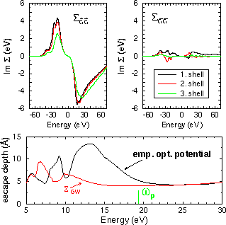 Fig. 1: Top: imaginary part of the GW self-energy of TiTe2. Shown are some diagonal (left) und off-diagonal elements (right) of the self-energy matrix in Fourier representation at the Gamma point. Bottom: calculated escape depth with this optical potential and with an empirical approach.
The modulus of the imaginary part turns out to be larger than in the
optical potentials used before. This has the immediate consequence of
increased surface sensistivity compared to previous calculations.
As a first application the mean free path or (electron) escape depth is
calulated with the old and the new optical potential. The higher surface
sensitivity is obvious from the reduced escape depth.
The self-energy reveals a strong increase in its
imaginary part above the
plasmon frequency. This smoothes the escape depth at high energies.
The main structure in the
escape depth occurs at lower energies and stems from the band structure.
To discuss the effects of the bands, which are seen here for the first
time, the escape depth is calculated for the GaAs(110) surface as shown in
the upper panel of Fig. 2. The discussion is easier for this surface
since here the bulk conduction band structure coincides nicely with the
energy vs. wave vector plot, the latter being obtained through a Fourier
transform of the
scattering states as can be seen in the lower
panel of Fig. 2. For TiTe2 there appear strong differences
in such a comparison.
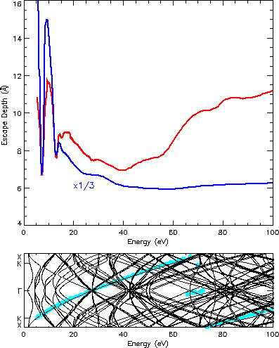 Fig. 2: Top: escape depth of GaAs(110) with two density functionals for the optical potential, using the valence charge density (black) and the full charge density (red), for normal incidence. For presentation purposes, the latter curve is reduced by a factor of 3 and then shifted upward to coincide again in the minimum at 7 eV. Below: bulk conduction band structure perpendicular to the surface with the dominating wave vector of the scattering state (blue).
The strong descant in the escape depth below the plasma frequency (15.8 eV)
are caused by gaps in the band structure as the comparison of the upper
with the lower panel in Fig. 2 shows. A bulk state for the given energy
is not allowed for the dominating wave vector and the electron
cannot penetrate deep into the crystal. Such effects of the band structure
are observed here for the first time. Previous calculations did not include
the band structure or the discrete lattice.
The calculations for GaAs are performed with a third kind of optical
potential. The self-energy is assumed as a function of the local
charge density in a
way similar to the procedure applied by the LDA for the exchange and
correlation in the ground state. The imaginary part of the self-energy is
calculated as a function of the local charge density.
The function is fitted to well known results for the homogenous electron
gas. Therefore the optical potential depends only on one position and the
energy. Several choices are possible for such a
function. For a valence density functional Fig. 3 shows the charge
density and the resulting optical potential for two energies.
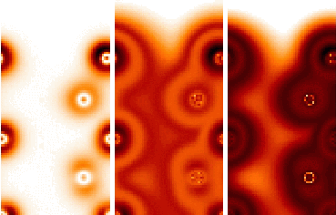 Fig. 3: Valence charge density (left) and optical potentials at 10 eV (middle) and 30 eV (right) of GaAs(110). Shown is a cut in direct space with the vacuum at the top of the images. Dark shades belong to high charge density and high damping. The optical potential from the local density functional shows more structure than the charge itself. This comes from the nonlinearity of the functional which gives strongest damping at mediate density. The spatial structure of the damping is important for electron spectroscopy by its influence on the spatial structure of the scattering state or, for photoemission, of the initial and final states.
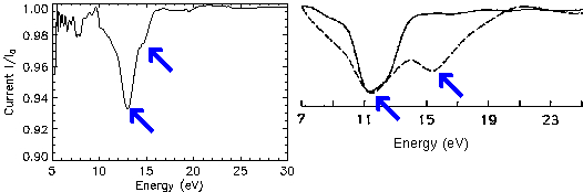 Fig. 4: target current spectra for GaAs(110). Left: this work, right: older KKR calculation (solid) and experiment (dashed).
As a byproduct the total current spectrum (TCS) was obtained for GaAs, see
Fig. 4. It confirms a previous suggestion about a second
experimental current minimum which has to be attributed to a second gap
in the band structure. However, it was not found through a VLEED
calculation with muffin-tin potentials as also shown in Fig. 4.
It is clearly a consequence of the electronic structure from the
pseudopotential used here.
See also:
|
 |