|
|
The electronic structure of cetineites |
![]()
|
Cetineites are members of a family of nanoporous crystals. In the field of
nanoporous materials the cetineites stand out for their photoconducting
properties. Other known nanoporous materials, including the ubiquitous
zeolites,
are insulators. Cetineites promise to add electrical control capabilities to
the technologically important properties of these materials.
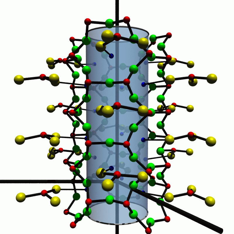
Cetineite minerals were first discovered in 1987 in Le Cetine mine in Tuscany, Italy, where they had grown due to natural weathering of the slags deposited by the antimony mine at the start of the 20th century. The creation of synthetic analogues of cetineites has been recently perfected by Liebau and Wang at the University Kiel and, in succession, by Simon and Jockel in Essen. The latter also have done extensive experimental characterizations of the cetineites they produced. We have investigated cetineites for the first time theoretically. The electronic structure was determined self-consistently and the results interpreted to propose a mechanism of conduction in the crystals. Particular attention was paid to the dependence of the optical gaps on the chemical composition. The trend found experimentally could be confirmed and explained. Cetineites have the general formula A6[Sb12O18][SbX3]2 (6-mx-y)H2O x[Bm+(OH)m] y¤ with A=Na+, K+, Rb+; X=S2-, Se2-; B=Na+, Sb3+; ¤ may stand for an unoccupied lattice site. The crystals have space group symmetry P63 or P63/m. In the structure tubes, as displayed in Fig. 1, are arranged in a hexagonal rod packing. The lattice constants are a=14.5 Å and c=5.5 Å. The tubes have a void of about 7 Å diameter. It is thought that the arrangement of electrically neutral [Sb12O18] tubes should be held together by ionic bonds between the [SbX3]3- pyramids and the A cations lining the tube walls. (For details see Liebau95, Wang95.)
Fig. 1: Perspective view of a single cetineite tube. The yellow spheres indicate the chalcogen X atoms which make up pyramids with antimony Sb shown in red. The green spheres are oxygen and the blue ones alkali A. Bonds thought to be covalent are drawn in thick lines while the ionic A-X bond is thin. The shaded cylinder shields the view of the atoms in the background to make seeing the structure simpler. The c axis runs from the bottom to the top of the picture. The computations have been done using the linear augmented plane wave (LAPW) procedure. From the self-consistent potential the density of states (DOS), band structure and dielectric function for members of the cetineite family with A=K,Na and X=S,Se are produced. The abbreviation (A;X) stands for A6[Sb12O18][SbX3]2 denoting the structure calculated. The ions Bm+ and the water molecules in the tubes are strongly disordered and have been left out of the calculations because of their minor importance and the computational burden. No effect on the electrical and optical properties has been detected in experimental investigations of several samples. Thus, there are included 44 atoms and one empty sphere per unit cell.
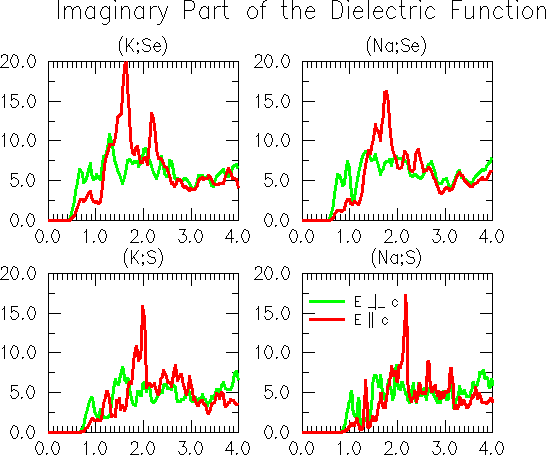
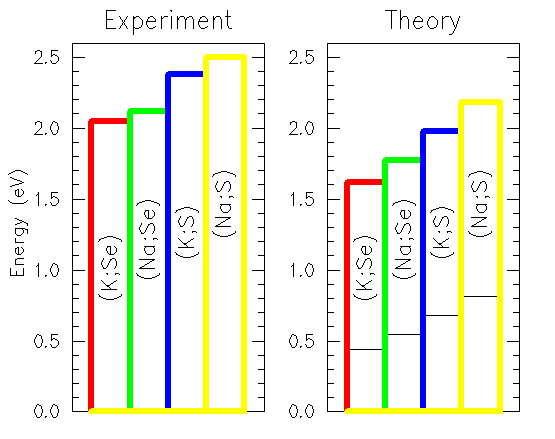
Fig. 2: Imaginary part of the dielectric function of the cetineites (K;Se), (Na;Se), (K;S) and (Na;S), as calculated by the LAPW technique. The photon energy in given in eV. Fig. 2 shows the imaginary parts of the dielectric functions of the four cetineites for which calculations were made. The high maximum in the calculated curves is a typical feature for all four compounds. Differing compositions (A;X) mainly cause a shift of the onset and the high maximum. Fig. 3 displays the chemical trend of calculated band gaps of the four members of the cetineite family. As usual in local density theory the gaps might be underestimated. Also the exact onset of both absorption and photoconductivity, is difficult to derive from the experimental data obtained at room temperature. We believe that one should rather consider the direct transition energy corresponding to the high maximum in the imaginary part of the dielectric function to account for the absolute values of the onsets.
Fig. 3: Experimental optical gaps (left, see Simon97 and Jockel98) and theoretical energies of maximum absorption (right, thick lines) together with the direct band gaps (thin black lines) dependent on the composition of the crystal.
Disregarding the uncertainty in the interpretation of the absolute values
the chemical trend itself shows excellent agreement with the experimental
results. It follows the ionization energy of the alkali atoms
which is larger for sodium than potassium, thus enhancing the binding energy
and thereby the gap for sodium. This is to be expected as the valence shell
of these atoms is completely ionized in all four compounds studied. The larger
gaps of the sulfur compounds as compared with the selenium ones confirm
the trend which is met in many covalently bound crystals containing these
elements, as e.g. the II-VI or III-VI compounds, and reflect most probably the
strength of the SbX3 binding in the outer pyramids.
To summarize we have
selfconsistently calculated the electronic structure and optical properties
of a most promising family of nanoporous compounds. It proves that such
calculations are not only feasible but offer essential physical insight into
the correlation between the geometry and chemical character of the bonds
on one hand, and the electronic structure on the other.
A remarkable difference of more than 1 eV between the calculated fundamental
band gap and the calculated pronounced maxima of absorption appears. The
latter coincides in energy with the observed onsets of photoconductivity and
absorption suggesting that the measurements at room temperature display the
pronounced
features of the dielectric function not resolving the fundamental gap.
The experimentally found chemical trend within a series of four
compounds could be theoretically reproduced and explained. This finding does
not depend on whether the size of the fundamental gap or the position of
maximum absorption is regarded.
See also:
|
1998 Frank Starrost
![]()
 |